Introduction to space-constrained applications
Space-constrained applications are increasingly common in the field of electronic devices. They require small and effective PCBs (printed circuit boards) to make them work within a limited space. Designing such PCBs is the role of hardware development services which are aimed at optimizing performance while following spatial constraints. Compact designs also enhance overall system efficiency and advanced embedded systems greatly benefit.
Maximizing space with compact designs
Designing compact PCBs is important for constrained-space applications. These designs enable more components to be fitted into smaller spaces, thereby making use of the available space effectively. Hardware development service can reduce the footprint of PCBs without sacrificing functionality through efficient layout techniques. In addition, this will save not only space but also the device’s overall weight hence suitable for portable and wearable technology.


Smaller and lighter terminal devices are more favourable to users, improving their convenience and operability. Optimal use of the space on the PCB means that all the components required for a particular application are incorporated without the wastage of space and this is manifest in medical devices, Smartphones, and fitness trackers.
Enhancing performance and reliability
Miniature and optimized printed circuit boards can improve the functionality and reliability of electronic goods. Through the careful placement of components and limiting the length of interconnecting linkages, signal integrity is enhanced thus reducing the effects of interference and noise. This leads to higher transfer rates and more dependable data communication, which is mandatory for sophisticated embedded systems.
Also, these miniature PCBs decrease power consumption, which in turn enhances the battery life of portable devices. Since they use less energy to operate, these devices become more efficient to use, which makes them suitable for use in applications where power needs to be conserved. The Compactness of PCBs also helps in adding features to small form factors where functionality can be increased without necessarily reducing performance.
These benefits are especially crucial in industries like the consumer electronics market, where the stability of the devices and their battery life are significant competitive factors. Optimizing PCB design therefore enables manufacturers to provide better technology as demanded in the current market.
Cost-effective manufacturing and assembly
The other advantage of designing compact and efficient PCBs is that their production and assembly cost are relatively less. Miniature PCBs need less material to make, thus cutting manufacturing costs. Second, efficient designs enable easy assembly, hence efficient and accurate production can be achieved. These aspects can be capitalized on by hardware development services to provide quality PCBs at an affordable price, thus being suitable for a range of applications.
Less raw materials consumed not only lower the cost but also improve the sustainability of the manufacturing processes since wastage is curbed. This reduces the time taken to assemble products hence lowering labor costs and minimizing the possibility of making mistakes, thereby improving efficiency. Such cost savings make it possible for companies to channel their resources in other crucial areas of growth and change thus enhancing their competitiveness in the market. Through the provision of small and powerful PCB solutions, hardware development services guarantee that appropriate and affordable electronics can be acquired for various industries today.
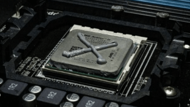
Improved heat dissipation
Effective thermal management is a key challenge in PCB design, especially for complex embedded platforms. Miniature and dense PCBs can also improve heat dissipation by positioning components strategically and including thermal vias and heat sinks. Heat control is crucial as excessive heat may adversely affect certain parts and cause the life of the gadget to be shortened. Optimization of these PCB designs facilitates proper heat dissipation hence proper working temperatures are maintained.
Thermal vias are implemented to dissipate heat through differently located layers of the PCB, sparing components. Heat sinks offer an additional route through which heat can be conducted, typically used with high heat-generating components to ensure stability. The positioning of these elements in a densely packed layout makes it possible for every component on the PCB hardware to stay within safe temperatures.
Read also: Understanding Naked Eye 3D Technology: How It Works, Applications, and Benefits
These improvements in heat dissipation are particularly beneficial to modern industries where advanced embedded systems are widely used, including automotive, telecommunications, and industrial automation. As a result of proper thermal control, small and dense PCBS have a direct positive impact towards the functionality and lifespan of complex electronic devices and systems.
Flexibility of the design and application
Miniature and dense PCBs have more design and application versatility than larger, less dense PCBs. They can be designed to meet certain specifications, and as such, are suitable for use in a range of fields including the healthcare sphere, aviation, and electronics. Outsourced hardware development services can then produce PCBs that will fit the various needs of each application and environment. This feature is especially valuable for high-end embedded systems that, as a rule, need individual approaches. Miniaturization and packaging of components along with putting many functions on a single PCB let the designers develop even more complex and dependable products.
Also, miniaturization of PCBs can minimize the size and mass of the end product which is essential in sectors that require size and weight saving such as in portable medical equipment and aerospace technology. The improved efficiency of PCBs also leads to improved thermal regulation and energy utilization, which increases the durability and functional capabilities of the devices to which they connect. Through employing the services of hardware development companies, organizations are guaranteed to get not only small and efficient PCBs but also durable ones developed to suit the needs of the business.
Supporting advanced embedded systems
Sophisticated embedded systems cannot be complete without proper arrangement of the PCBs they use. These systems are typically located in areas where space is very limited as each millimeter is crucial. Miniature and high-density PCBs allow more functions and functionalities to be incorporated in small areas. This integration is necessary for applications, for example, IoT devices in which size and performance are critical. Thus, using effective printed circuit boards, and hardware development services can meet the increasing needs of highly integrated embedded systems.
Conclusion
To sum up, the benefits of designing small and powerful PCBs for smaller space applications are numerous. These designs maximize occupancy of space, improve performance and dependability, lower manufacturing costs, better heat dissipation, aid in design variety and facilitate advanced embedded system. These benefits are achieved through hardware development services that aim at tailoring electronic gadgets to meet the highly dynamic needs of diverse sectors. By concentrating on compact and efficient PCB designs alone can manufacturers create inventive products capable of excelling in cramped spaces.